
New Camera Project
I recently bought an old Spectral Instruments 600 series camera for a very low price on ebay. Before I bought it I didn't even know which CCD sensor it had, as the 600 series was offered with four standard CCD options (e2v CCD42-40, Kodak KAF-16800, Tektronix TK1024 and the SiTE SI-003) and also other compatible CCDs as a custom request. The KAF-16800 would have been ideal due to its large size and higher resolution, but it ended up having the next best option of the e2v CCD42-40 - this seems to be the most common sensor option for the 600 series.
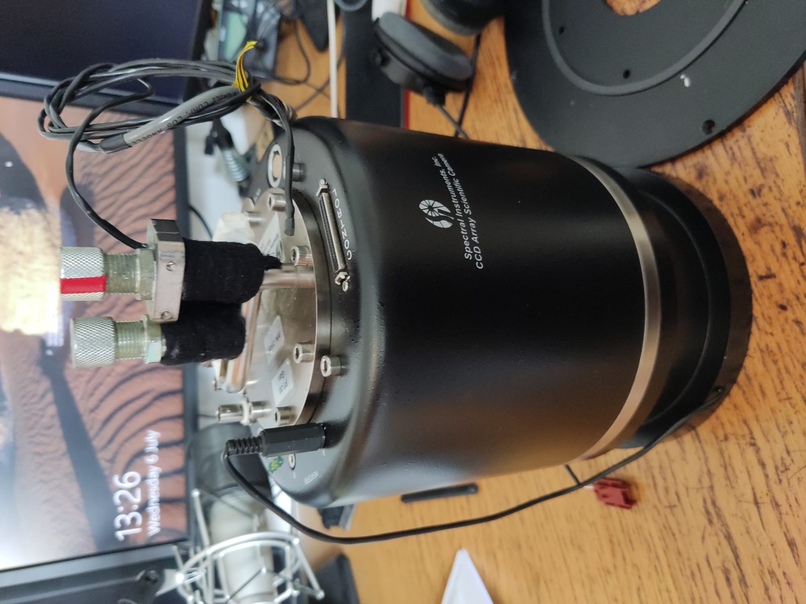
Spectral Instruments 600 camera.
The CCD specifically appears to be the AIMO back illuminated version. Unfortunately I can't find any indication of the coating but I would guess either the midband or broadband AR coatings - both options have very good QE across the red and green parts of the spectrum, with the midband having a typical QE over 90% for H-alpha and OIII.
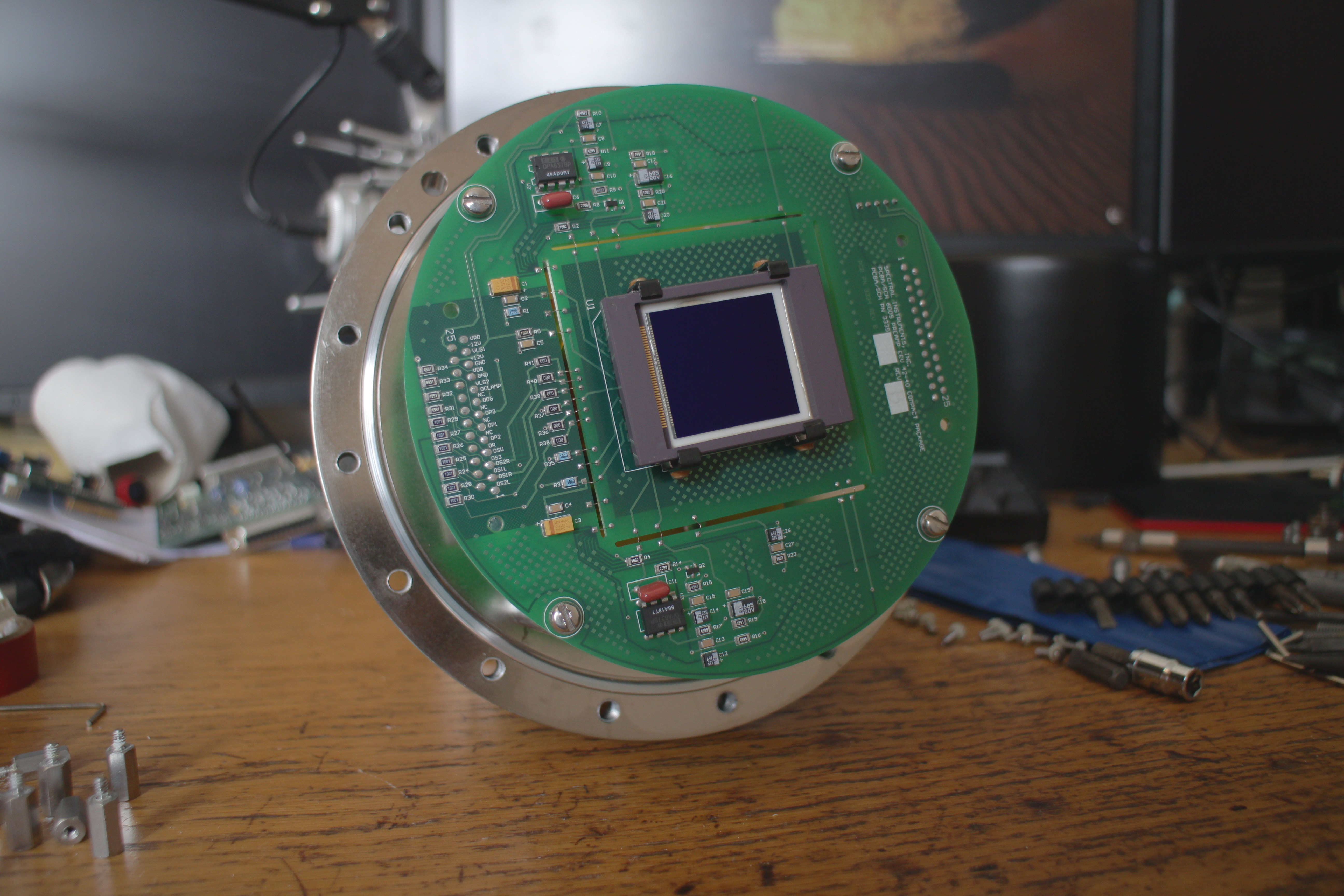
The e2v CCD42-40 CCD sensor. [Full resolution]
My past CCD camera designs have used the 16-bit AD9826 ADC as an analog front end, a very convenient IC for CCD cameras, having a built in programmable preamp and correlated double sampling. Unfortunately its noise performance isn't great, measuring at around 3.5 ADU RMS self noise in my tests. If used at a gain of around 0.6e-/ADU, covering the full well depth of the CCD42-40, this would correspond to around 5.34e- RMS of read noise just from the ADC alone. The CCD42-40 datasheets specify a minimum typical read noise of around 3e- RMS using a clamp and sample CDS method. Better sampling techniques could likely provide even better results, meaning the AD9826 would be the limiting factor for read noise.
In order to get the best performance I'll be rolling my own CDS implementation for this camera. Of the 3 main methods clamp and sample seems to be the worst option for noise performance, as white noise can't be filtered out well without significantly limiting preamp bandwidth, typically leading to settling times being far too long. Digital multisampling and dual slope methods both look ideal for this camera, both being able to provide similar noise performance.
Below is a rough schematic for a potential dual slope CDS implementation. The first stages will be located on the same board as the CCD, starting with an emitter follower. The CCD42-40 suggests using either a resistor or constant current source as a load for the source follower output of the CCD's amplifier. Since the source follower's gain and bandwidth will vary with output current, using a constant current source should provide better linearity. The emitter follower configuration in this design is simple and the change in current over the full output range of the CCD is an order of magnitude lower than simply using a resistor as a load. Care should be taken to avoid the transistor from oscillating - keep the everything tightly layed out and routed to avoid parasitic inductance. A small value resistor or ferrite bead can be added in series before the transistor base to further suppress oscillations.
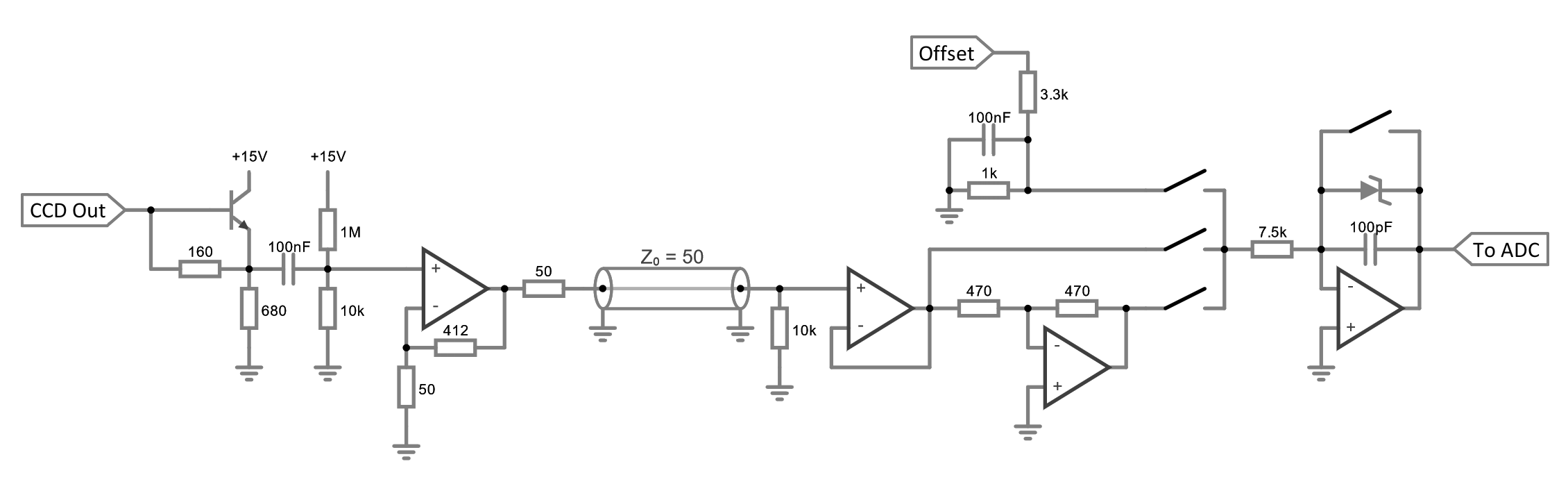
Rough dual slope CDS implementation schematic. [Full resolution]
Noise of the emitter follower will largely be determined by collector current shot noise and base spreading resistance. Collector current with the resistor values shown is around 7.5mA, corresponding to a noise density of approximately 0.17nv/rtHz. This can be kept below 0.5nv/rtHz by selecting a transistor with a base spreading resistance below ~13 ohms. Unfortunately very few transistor datasheets specify base spreading resistance, however there are a few sources online with measurements. Most seem to agree the the ZTX series are among the most promising, with the ZTX851 looking like the most ideal candidate - having a typical rbb' of below 2 ohms.
This stage is followed by an op-amp in a non-inverting configuration. Gain in this stage is not critical, however noise performance of later stages will benefit from this being reasonably high. Op amp should be selected for a low input noise density, high bandwidth, high slew rate and very low settling times. Op amp output has 50 ohm series termination, and is then sent over a transmission line (probably coax with U.FL connectors) to the next board.
Input impedance of the next section should be high, this intentially creates a reflection coefficient of close to 1, which is ideal for the series termination configuration of the preamp. In any case the transmission line will likely be short (<10cm), well below the wavelength of the CCD output amplifier bandwidth.
Correlated double sampling is achieved by an inverting amplifier and an analog multiplexer or SPST analog switches. The switch from the inverting amplifier should be closed for the reference sample, the switch from the non-inverting amplifier should then be closed for an equal amount of time for the signal sample. The offset switch can be closed for a small amount of time to add an analog offset, since the switch on time cannot be controlled with high precision by a microcontroller, the offset supply will be varied by a DAC instead, a small 8 to 12 bit DAC followed by an inverting amplifier should be ideal for this.
A zener diode is used in series with the integrator's capacitor. This clamps the output, preventing it from going a diode drop below GND and the zener voltage above GND. This can be used to ensure the output is not too far out of range to damage the ADC inputs.
A brief look at some ADCs and the AD4630-24 looks like an ideal candidate. 2 channels with simultaneous sampling, high bit depth, low noise and good linearity - only downside is the hard to solder BGA package, though it does have a fairly nice pad layout and some integrated bypass capacitors making layout on a 4 layer board easy.
Various Die Shots
VV5351 optical mouse sensor from IntelliMouse Optical 1.1A under reflected darkfield illumination. This sensor often gets incorrectly referred to as an 'MLT04' online due to the markings on top of the package - MLT being a country code referring to ST's assembly plant in Kirkop, Malta. The correct part number (VV5351) is found on the reverse side of the package.
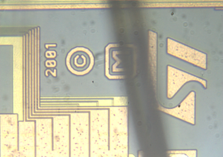
VV5351 ST logo markings.
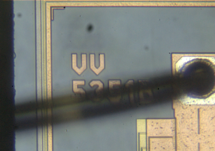
VV5351 part number markings. Die shows VV5351B but package markings showed VV5351A, most likely the package tooling wasn't updated to save costs.
Texas Instruments 74LS32.
MCP3201 (12-bit ADC).
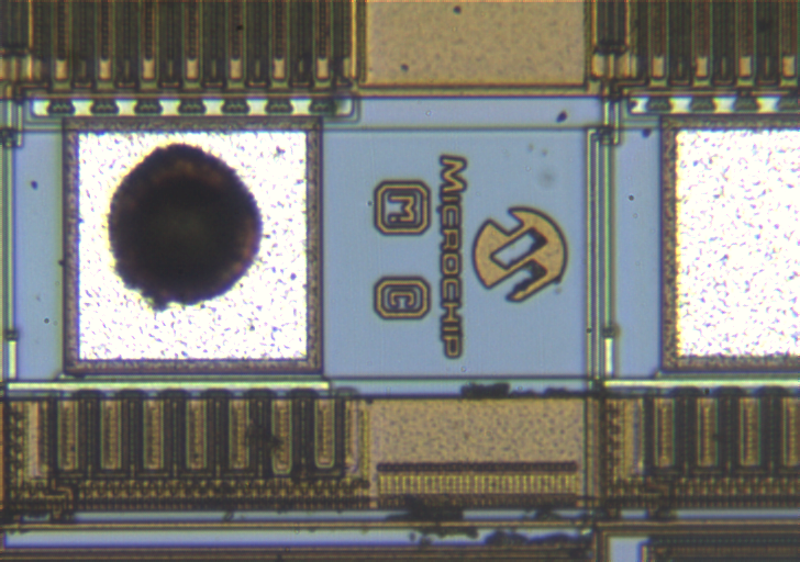
MCP3201 Microchip logo markings.
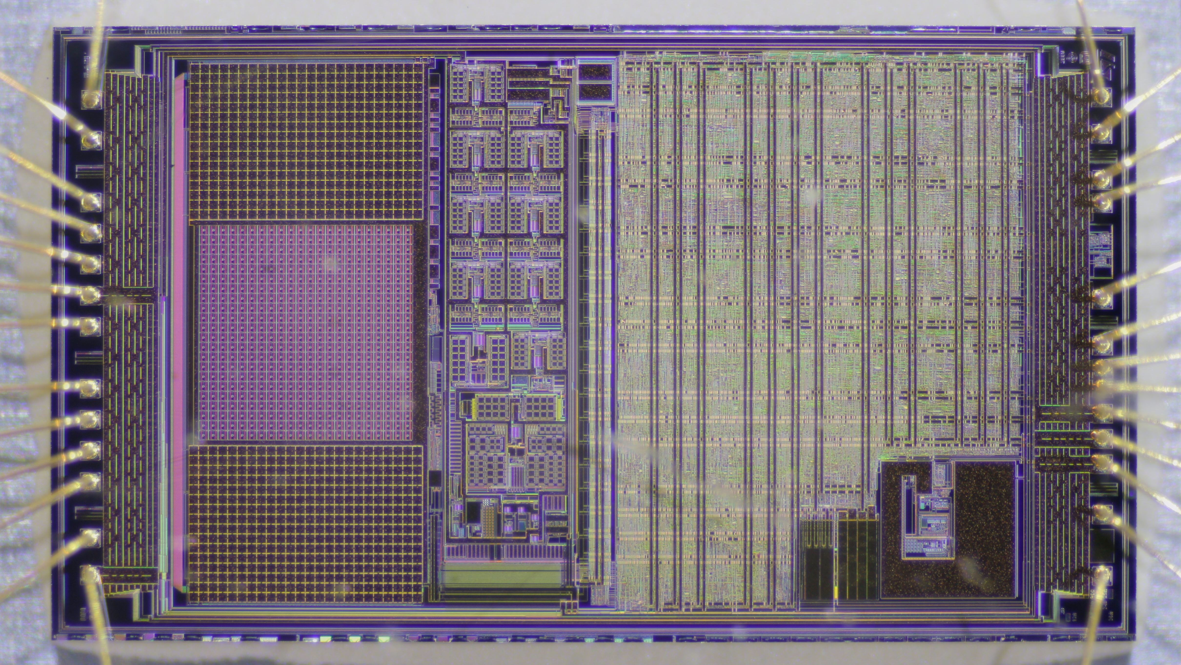
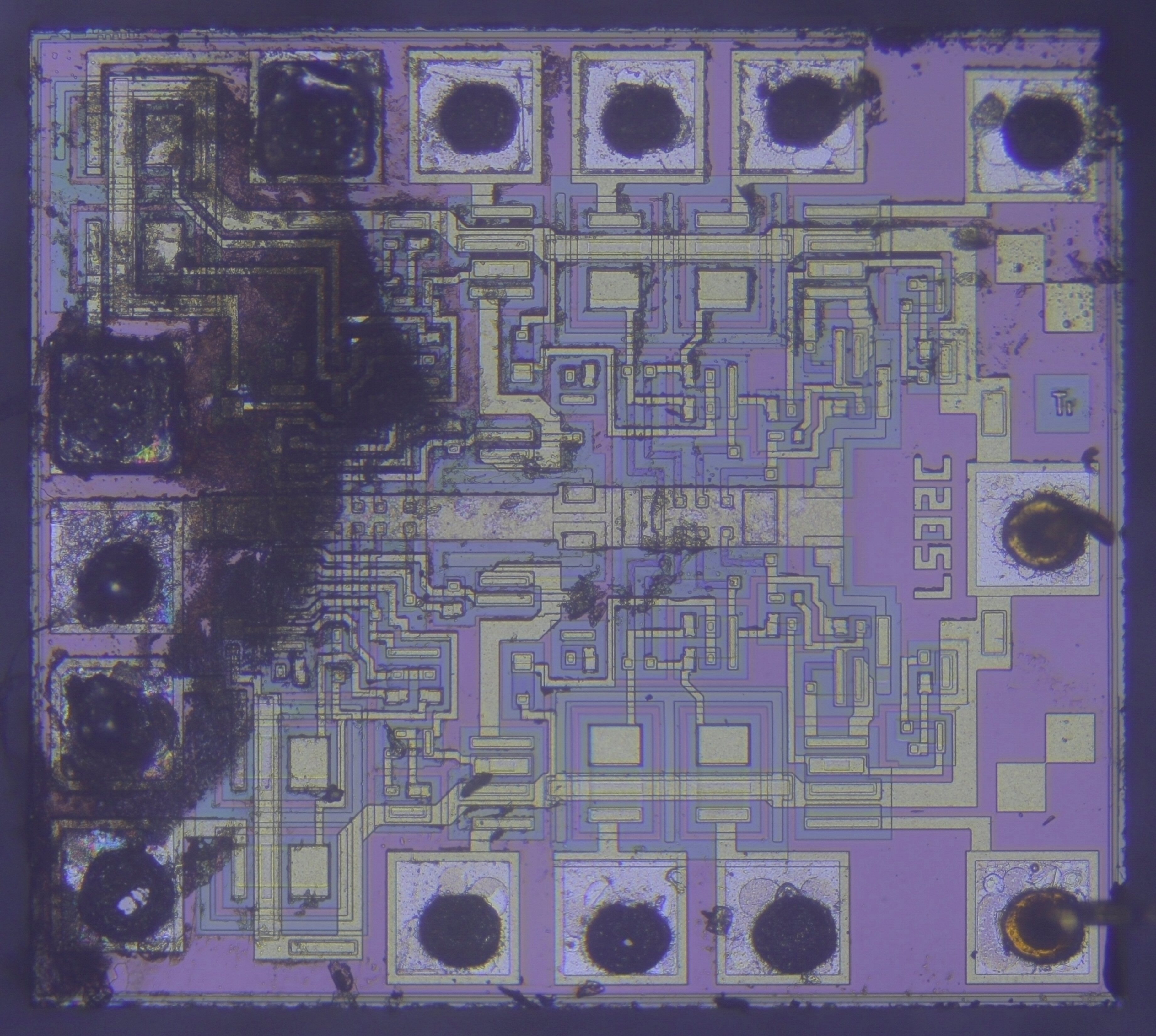
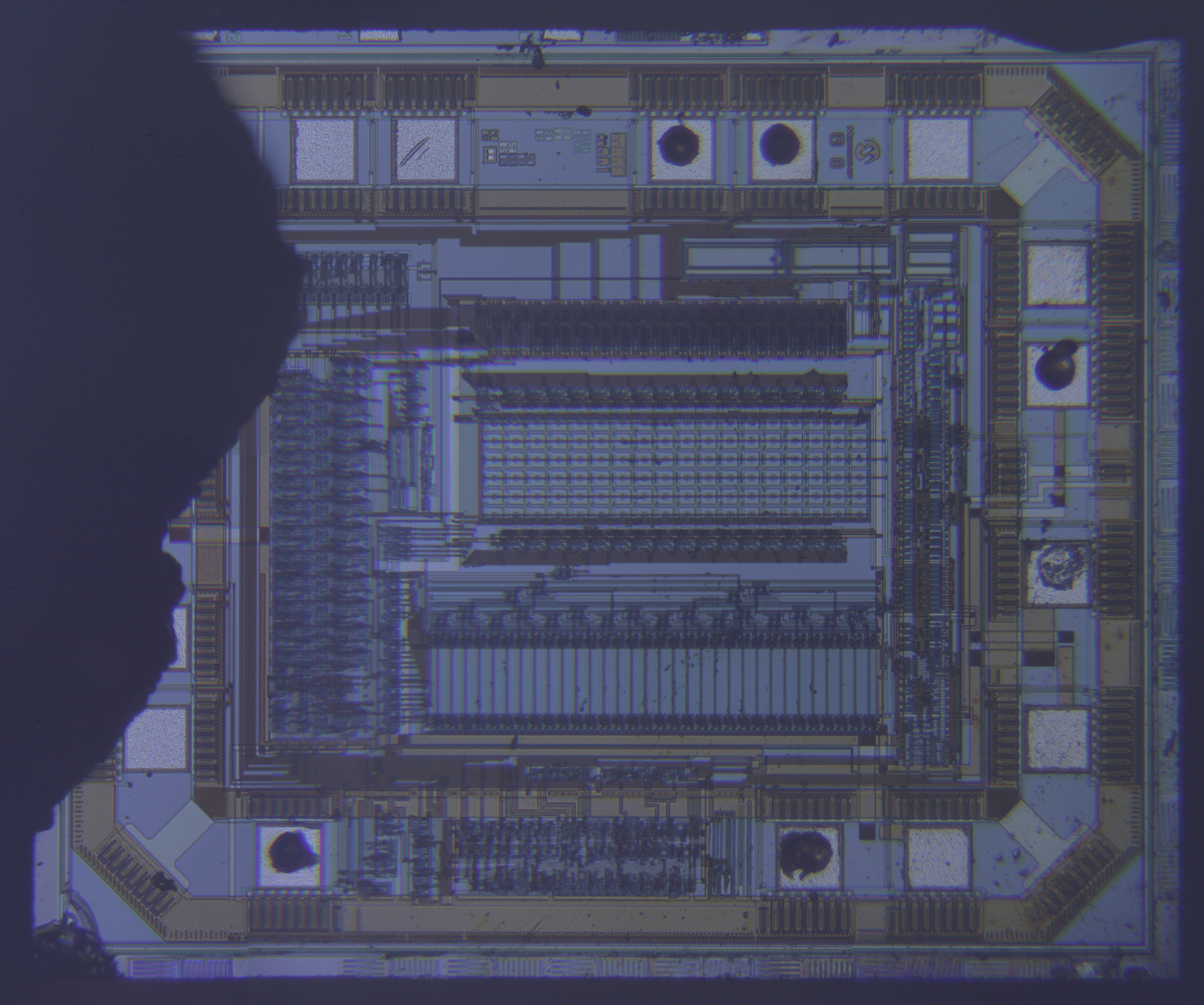
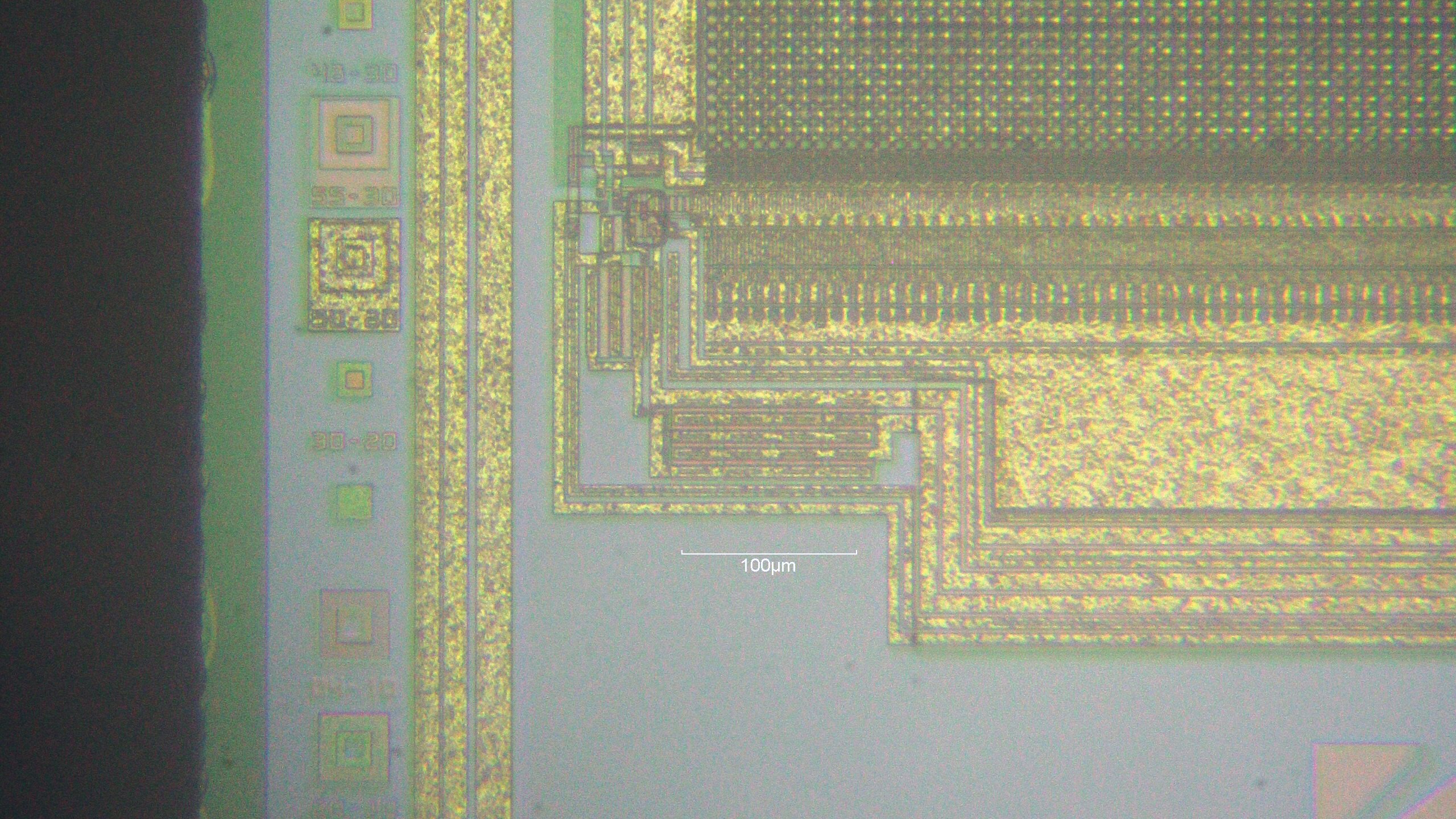
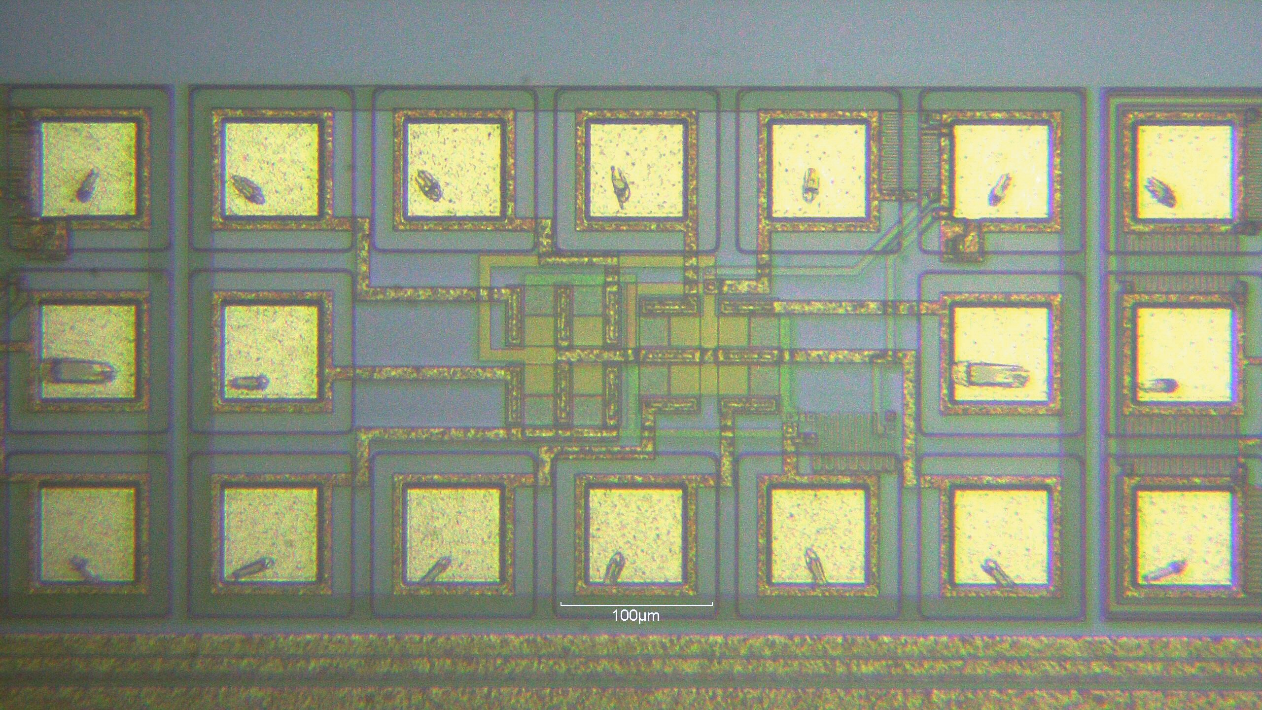
KAI-11002 Die Shots
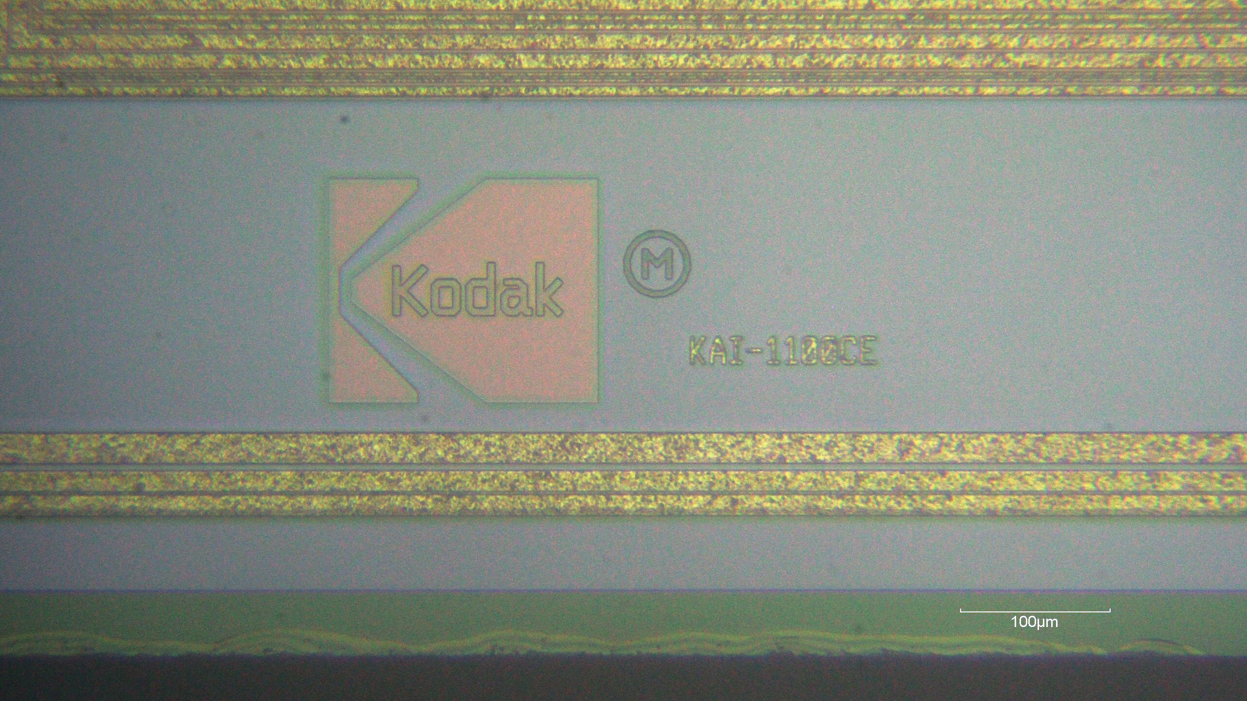
Kodak logo die marking.
Floating diffusion, output gate and output amplifier structure. Mask alignment structures on the left edge.
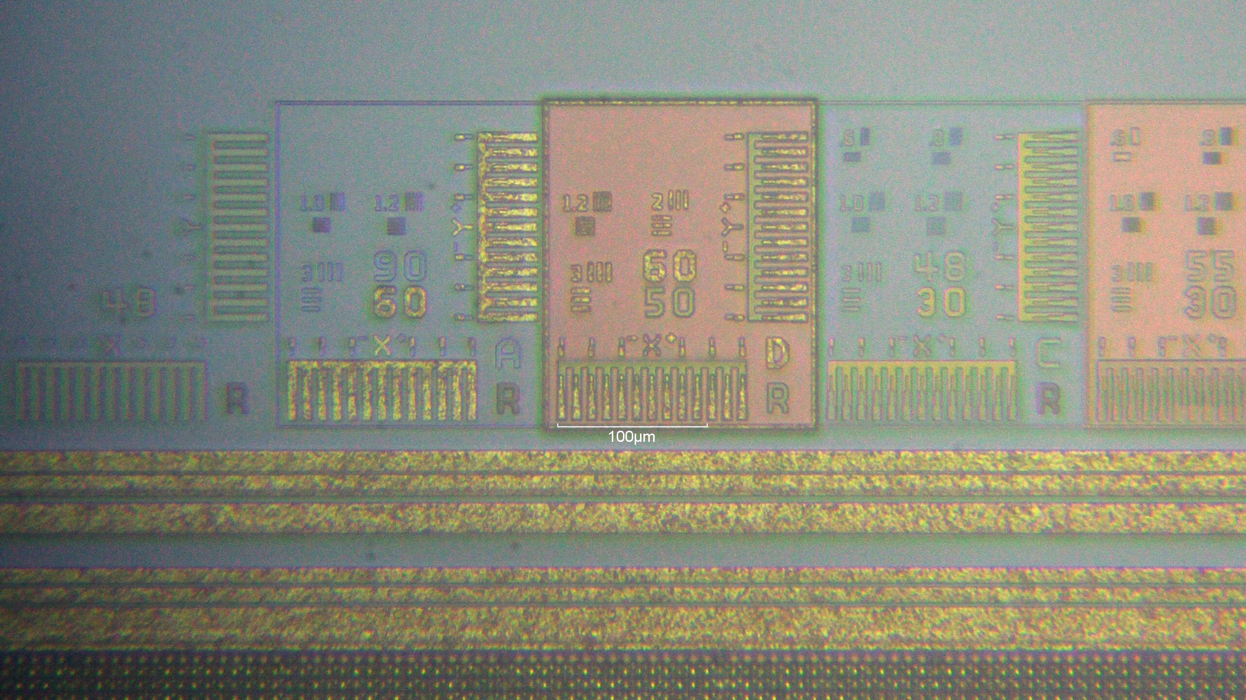
Active test structures on the border of the die.
Test areas to measure mask scale and distortion.